• Data center & Networking Equipment
• Servers/Storage Devices
• High Performance Computing (HPC)
• Switches/Routers
• Telecom Central Offices (CO)
• Test and Measurement Equipment
Features
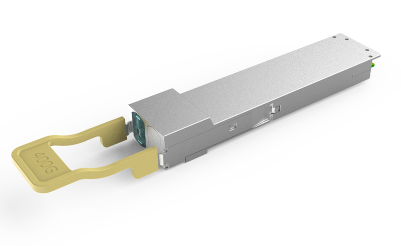
• Hot-pluggable OSFP 400G SR4 multimode transceiver
• Compliant with OSFP RHS
• Compliant with CMIS Rev 5.0 and above revision
• 4-channels of 100G-PAM4 electrical and optical modulation
• Maximum power consumption 8.5W with 4 channels and 6.5W with 2 channels
• Single MPO-12 APC receptacles
• Up to 30m reach on OM3 and 50m reach on OM4
• Operates as a 200Gb/s NDR200 transceiver with 2-fiber splitter ends
• Case operating temperature 0°C to 70°C
Product Specification
Absolute Maximum Ratings (TC=25℃, unless otherwise noted
Stresses in excess of the absolute maximum ratings can cause permanent damage to the device. These are absolute stress ratings only. Functional operation of the device is not implied at these or any other conditions in excess of those given in the operational sections of the data sheet. Exposure to absolute maximum ratings will cause permanent damage and/or adversely affect device reliability.
Parameter | Symbol | Min | Typical | Max | Unit | Notes |
Storage Temperature | TS | -40 | - | +85 | ℃ |
|
Maximum Supply Voltage | Vcc | -0.5 | - | 3.6 | V |
|
Operating Relative Humidity | RH | 5 | - | 95 | % | No condensation |
Control Input Voltage | VI | -0.3 | - | VCC+0.5 | V |
|
General Specifications (Tc=25℃, unless otherwise noted)
Parameter | Symbol | Min | Typical | Max | Unit | Notes |
Operating Case Temperature | TOPR | 0 | - | 70 | ℃ |
|
Power Supply Voltage | VCC | 3.135 | 3.3 | 3.465 | V |
|
Instantaneous peak current at hot plug | ICC_IP | - | - | 3600 | mA |
|
Sustained peak current at hot plug | ICC_SP | - | - | 3000 | mA |
|
MaximumPower Dissipation(400G) | PD | - | - | 8.5 | W |
|
Maximum Power Dissipation(200G) | PD | - | - | 6.5 | W |
|
Maximum Power Dissipation, Low Power Mode | PDLP | - | - | 1.5 | W |
|
Signaling Rate per Lane | SRL | - | 53.125 | - | GBd | PAM4 |
Two Wire Serial Interface Clock Rate | - | -100 | - | 400 | kHz |
|
Power Supply Noise Tolerance (10Hz - 10MHz) | - | - | - | 66 | mV |
|
Rx Differential Data Output Load | - | - | 100 | - | Ohm |
|
Operating Distance (OM3) | - | 2 | - | 30 | m |
|
Operating Distance (OM4) | - | 2 | - | 50 | m |
|
Transmitter Characteristics (TC=25℃, unless otherwise noted)
Parameter | Symbol | Min | Typical | Max | Unit | Notes |
Wavelength | λC | 844 | 850 | 863 | nm |
|
RMS spectral width | ∆λrms |
|
| 0.6 | nm |
|
Average Launch Power, each lane | AOPL | -4.6 | - | 4.0 | dBm | 1 |
Outer Optical Modulation Amplitude (OMAouter), each lane | TOMA | -2.6 |
| 3.5 | dBm | 2 |
Transmitter and Dispersion Eye Closure for PAM4 (TDECQ), each lane |
TDECQ |
- |
- |
4.4 |
dB |
|
Average Launch Power of OFF Transmitter, each lane | TOFF | - | - | -30 | dBm |
|
Extinction Ratio, each lane | ER | 2.5 | 3.5 | - | dB |
|
RIN14OMA | RIN | - | - | -132 | dB/Hz |
|
Optical Return Loss Tolerance | ORL |
| - | 12 | dB |
|
Transmitter Reflectance | TR | - | - | -26 | dB | 3 |
Notes
1. Average launch power, each lane (min) is informative and not the principal indicator of signal strength.
2. Even if max (TECQ, TDECQ) < 1.8dB, OMAouter (min) must exceed this value.
3. Transmitter reflectance is defined looking into the transmitter.
Receiver Characteristics (TC=25℃, unless otherwise noted)
Parameter | Symbol | Min | Typical | Max | Unit | Notes |
Wavelength | λC | 842 | 850 | 863 | nm |
|
DamageThreshold,average optical power, each lane | AOPD | 5 | - | - | dBm |
|
Average Receive Power, each lane | AOPR | -6.3 | - | 4.0 | dBm |
|
Receive Power (OMAouter), each lane | OMAR | - | - | 3.5 | dBm |
|
Receiver Reflectance | RR | - | - | -26 | dB |
|
Receiver Sensitivity (OMAouter), each lane | SOMA | - | - | -4.4 | dBm | 1 |
StressedReceiverSensitivity (OMAouter), each lane | SRS | - | - | -1.8 | dBm | 2 |
Conditions of stressed receiver sensitivity test |
Stressed eye closure for PAM4 | SECQ |
| 4.4 |
| dB |
|
OMAouter of each aggressor lane | OMAouter |
| 3.5 |
| dBm |
|
Notes
1. Receiver sensitivity (OMAouter), each lane (max) is informative and is defined for a transmitter with TDECQ<=1.8 dB
2. Measured with conformance test signal at TP3 for the BER = 2.4x10⁻⁴
PIN Descriptions

Figure 1 – OSFP module Pinout
PIN | Logic | Symbol | Name/Description |
1 |
| GND | Ground |
2 | CML-I | TX2p | Transmitter Data Non-Inverted |
3 | CML-I | TX2n | Transmitter Data Inverted |
4 |
| GND | Ground |
5 | CML-I | TX4p | Transmitter Data Non-Inverted |
6 | CML-I | TX4n | Transmitter Data Inverted |
7 |
| GND | Ground |
8 | CML-I | TX6p | Transmitter Data Non-Inverted |
9 | CML-I | TX6n | Transmitter Data Inverted |
10 |
| GND | Ground |
11 | CML-I | TX8p | Transmitter Data Non-Inverted |
12 | CML-I | TX8n | Transmitter Data Inverted |
13 |
| GND | Ground |
14 | LVCMOS-I/O | SCL | 2-wire Serial interface clock |
15 |
| VCC | +3.3V Power |
16 |
| VCC | +3.3V Power |
17 | Multi-Level | LPWn/PRSn | Low-Power Mode / Module Present |
18 |
| GND | Ground |
19 | CML-O | RX7n | Receiver Data Inverted |
20 | CML-O | RX7p | Receiver Data Non-Inverted |
21 |
| GND | Ground |
22 | CML-O | RX5n | Receiver Data Inverted |
23 | CML-O | RX5p | Receiver Data Non-Inverted |
24 |
| GND | Ground |
25 | CML-O | RX3n | Receiver Data Inverted |
26 | CML-O | RX3p | Receiver Data Non-Inverted |
27 |
| GND | Ground |
28 | CML-O | RX1n | Receiver Data Inverted |
29 | CML-O | RX1p | Receiver Data Non-Inverted |
30 |
| GND | Ground |
31 |
| GND | Ground |
32 | CML-O | RX2p | Receiver Data Non-Inverted |
33 | CML-O | RX2n | Receiver Data Inverted |
34 |
| GND | Ground |
35 | CML-O | RX4p | Receiver Data Non-Inverted |
36 | CML-O | RX4n | Receiver Data Inverted |
37 |
| GND | Ground |
38 | CML-O | RX6p | Receiver Data Non-Inverted |
39 | CML-O | RX6n | Receiver Data Inverted |
40 |
| GND | Ground |
41 | CML-O | RX8p | Receiver Data Non-Inverted |
42 | CML-O | RX8n | Receiver Data Inverted |
43 |
| GND | Ground |
44 | Multi-Level | INT/RSTn | Module Interrupt / Module Reset |
45 |
| VCC | +3.3V Power |
46 |
| VCC | +3.3V Power |
47 | LVCMOS-I/O | SDA | 2-wire Serial interface data |
48 |
| GND | Ground |
49 | CML-I | TX7n | Transmitter Data Inverted |
50 | CML-I | TX7p | Transmitter Data Non-Inverted |
51 |
| GND | Ground |
52 | CML-I | TX5n | Transmitter Data Inverted |
53 | CML-I | TX5p | Transmitter Data Non-Inverted |
54 |
| GND | Ground |
55 | CML-I | TX3n | Transmitter Data Inverted |
56 | CML-I | TX3p | Transmitter Data Non-Inverted |
57 |
| GND | Ground |
58 | CML-I | TX1n | Transmitter Data Inverted |
59 | CML-I | TX1p | Transmitter Data Non-Inverted |
60 |
| GND | Ground |
Mechanical Specifications
Figure 2 – Mechanical Dimensions
Figure 3 – Active fiber ports in MPO12 connector on module side
Product Information
Data Rate | Factor | Optical | Wavelength | Reach |
400G | OSFP | SR4 | MPO | 850nm | 70m |
ESD Safety Cautions
This transceiver is specified as ESD threshold 1KV for high speed data pins based on Human Body Model per ANSI/ESDA/JEDECJS-001. The units are subjected to 15kV air discharges during operation and 8kV direct contact discharges to the case. However, normal ESD precautions are still required during the handling of this module. This transceiver is shipped in ESD protective packaging. It should be removed from the packaging and handled only in an ESD protected environment.
Important Notice
The performance figures, data, and any illustrative material presented in this datasheet are typical and must be explicitly confirmed in writing by ZHAOLONG before they are deemed applicable to any specific order or contract.
By ZHAOLONG's policy of continuous improvement, specifications may change without prior notice. The publication of information in this datasheet does not imply exemption from patent or other protective rights held by ZHAOLONG or other parties. Additional details can be obtained from any ZHAOLONG sales representative.
Revision Record
Rev. | Comments | Author | Date |
A01 | Initial Release | James Chen | 10/01/2023 |
|
|
|
|
|
|
|
|
|
|
|
|

 English
 简体中文
简体中文